Katana Hacking
Introduction
Here is a 1999 Suzuki GSX750F Katana with a 4-cylinder inline engine just beneath the cowling. Most of this engine’s control is purely mechanical. Rather than modern, electronically-controlled fuel injectors it has carburetors with a cable-controlled throttle body.
The only part of the engine that is computer-controlled is the ignition. For a gasoline engine to run, spark plugs need to ignite the fuel-air mixture in the cylinders at the right moment. In the case of this Katana, a microcontroller controls MOSFETs that trigger coils that power its spark plugs.
The board that holds this microcontroller, the MOSFTs, and supporting electronics is hidden in this box referred to as the ignition control system:
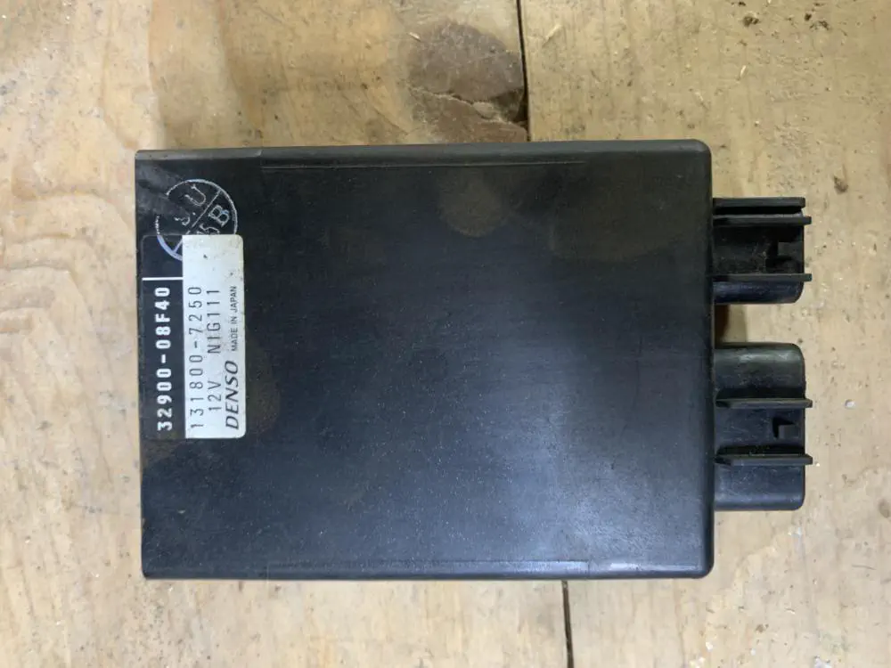
Timing the spark plugs requires this box to constantly know the rotation of the camshaft. To further complicate matters (and the reason a computer is being used), the optimal timing of ignition relative to the camshaft position changes depending on the engine RPM, throttle, and whether or not the Katana is even in gear.
Our goal is to figure out what is in this box, determine the microcontroller in use, and hopefully reverse engineer how this box is taking those inputs and generating these outputs.

Why Though?
The motivations behind this project are purely for fun:
- Reverse engineering microcontrollers is cool.
- Patching an ignition control system lets us tune the engine behavior:
- We can increase the horsepower by advancing the spark timing a few degrees.
- We can modify where the engine’s rev limit is (probably a bad idea though).
Deconstruction and Potting
People have already researched Suzuki GSXRs from similar years and those ignition control systems had BDM (Background Debug Mode) pins that could be used to dump the firmware on the chips. My plan was to try something similar.
I saw a video where someone was repairing some 1980s Katana ignition control systems. The person in the video simply removed the circuit board from the box. I assumed my experience would be the same so I started digging into the side opposite the connector.
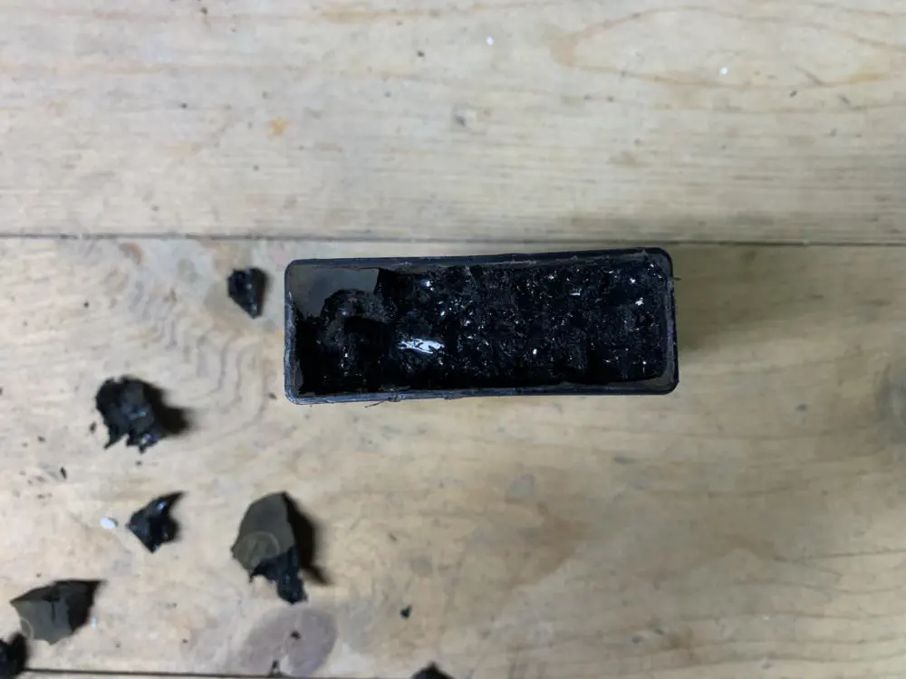
It looks like there’s some sort of sealant. That’s fine, as long as it’s not the entire box.
 Oh no.
It makes sense that Denso would seal their electronics by “potting” them. This seals away moisture as well as dampens vibrations. However, what is happening here is also intentional anti-reverse engineering. See those crystaline rock-like objects? Rather than simply using a sealant, they have mixed in these hard objects making it difficult to scrape away the sealant. In the process you end up damaging the board itself. Which is exactly what I did. I damaged some capacitors and the system stopped working, but as long as the microcontroller is still intact maybe I can at least dump the firmware.
And here it is, some sort of microcontroller next to what appears to be a 10 MHz crystal:
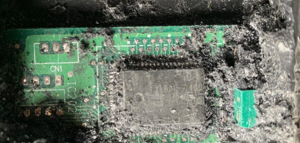
Awesome! It’s labeled 131850-1400 and appears to have a Denso logo on it. I could not find anything online for that part number though so let’s come back to that after we find some debug pins.
…
Well I’m still not seeing anything obvious, but see those eight pads labeled IC202 near the top of the image? 8 pins is a common number for a BDM port and maybe the IC label is there just to throw me off.

Brute-Forcing BDM Combinations
Since there’s no labeling on any of these pins let’s try to at least find a positive supply and ground on the board. One of the other components I was able to identify on the board was a Toshiba TA78DS05. This is a 5V voltage regulator and gives me a starting point for identifying positive and ground pins on the board by using the continuity tester on my multimeter.
Back to the IC202 pads, the lower left was ground and the lower right was the 5v output from the voltage regulator (the regulator was outputting to some of the pins on the microcontroller too). BDM often includes power and ground from the host to power the microcontroller directly. Maybe I can use an Arduino to try BDM protocols using different pin combinations on the other 6 unidentified pins?
After a few days trying this, I had no luck. I finally used my trusty Digilent Analog 2 to probe the ports and found that the only interesting port was the upper left pin which seemed to be outputting a 1.2 kHz square wave. Well this is bad news, I don’t know of any debugging protocols where the microcontroller is sending a clock OUT to the host. That along with the fact this is clearly labeled IC means this is probably some sort of supporting microcontroller, angle sensor, or external memory that was used in other versions of this board with the same PCB, but not this one.

Let’s try the back instead.
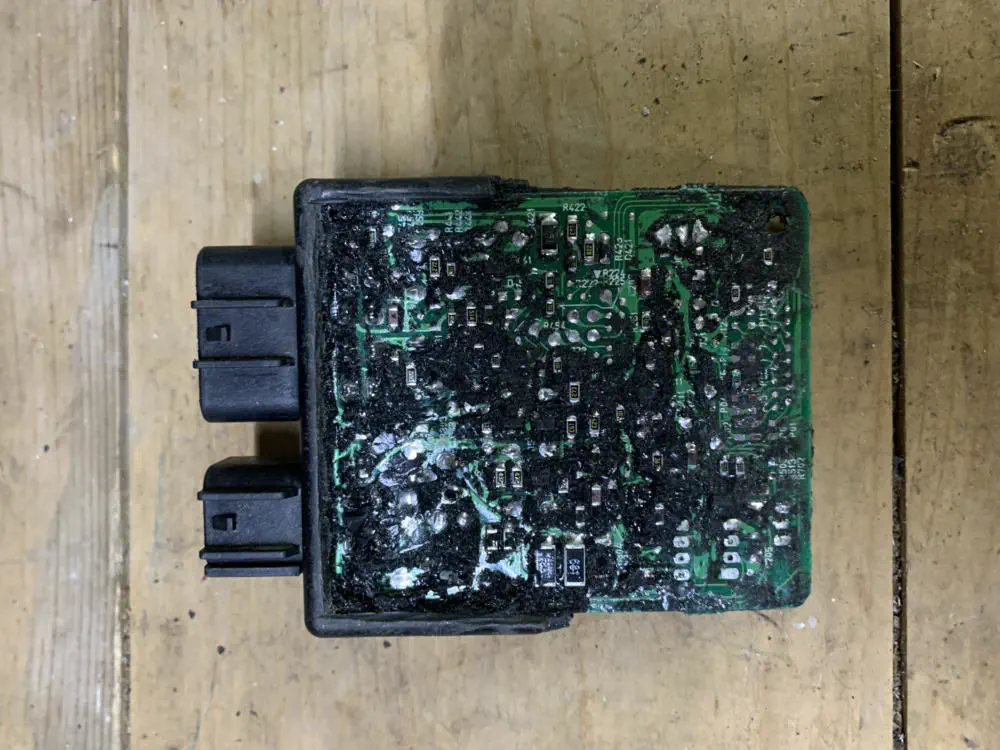
Yet another dead end! So there isn’t a debug port that I can see, we can’t identify the microcontroller from its part number, and I’m covered in pieces of sealant and rock things.

Identifying an Unknown Chip
This looks bad, but let’s go back to the microcontroller part itself. It is labeled as Denso 131850-1400, but I’m pretty confident Denso does not manufacture microcontrollers. That leaves us with two options:
A. It is an FPGA (Field-Programmable Gate Array) instead of being a microcontroller at all.
B. It’s a microcontroller that Denso ordered from another company and requested their “D” logo and part number be printed on it instead.
Option A is possible, it turns out FPGAs have been around since the 1980s and one could definitely be used to control the ignition. They are also really expensive compared to microcontrollers though so probably not. Option B sounds weird, but this actually happens frequently. It might help Denso track chips that have been flashed with their own code better and it certainly makes reverse engineering harder (which we already know Denso likes to do).
Assuming option B is the case, here is what we know:
- The microcontroller is in a 19x13 package (64 pins total).
- Vdd is pin 58 and Vss is pin 26 (using the continuity tester and 5V regulator).
- The 10 MHz crystal is outputting to pins 24 and 25 (using the oscilloscope and following the traces).
- We haven’t identified an external EEPROM chip anywhere on the board so the controller must have internal memory.
- We know that this chip was manufactured starting on or before 1999 because it can’t be newer than the Katana it came from.
I then spent a few hours Googling with the time set to “Before Jan 1, 2005”. Unfortunately, I just never managed to find a satisfactory answer from trying to match those parameters to a specific product.
Microscope Time
Although manufacturers are typically happy to put a different company’s logo on one of their products if they order at scale, they won’t change the physical die inside of the epoxy packaging. This means if we can successfully remove the epoxy (a process called decapsulation) and get to the physical silicon, we may be able to see the real vendor stamped into the die. This is, of course, a much more destructive process so I ordered a few identical ECUs from eBay and used a process called thermal decapsulation on the unknown chip.
After a few failed attempts I got an intact die and put it underneath a microscope:
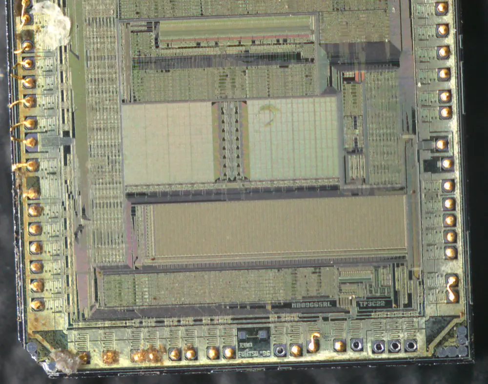
Okay so maybe it’s not fully intact, but anyway we finally get the answer we are looking for:
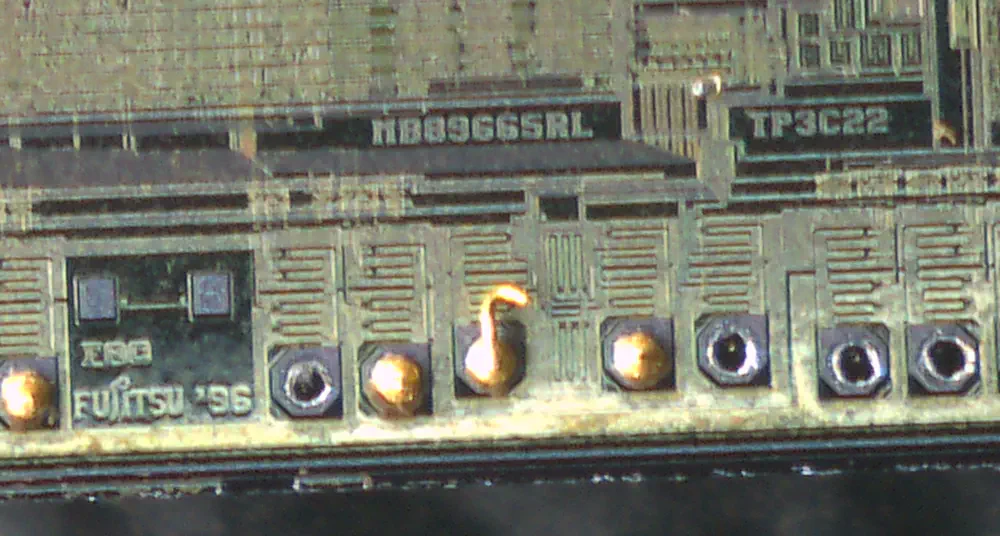
It’s a FUJITSU MB89665RL:
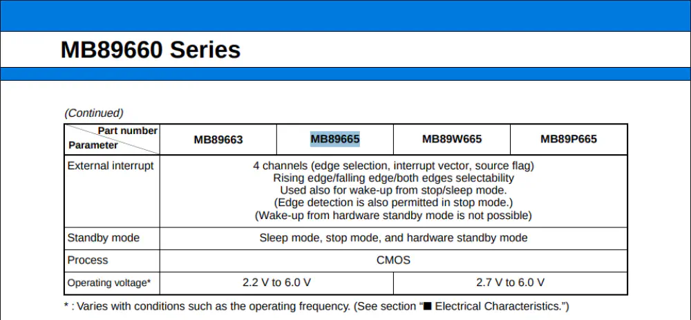
So unfortunately this microcontroller has mask ROM. This is a lot less common nowadays, but it means the program is built into the chip directly from the factory. If the microcontroller had external memory we could read it, if the microcontroller had reprogrammable memory we could read it. Much to my dismay, this is the only possibility where there’s simply no way to read the program without a high-quality metallurgical microscope and additional techniques to die the mask and read the bits optically. I do have a microscope, but it is not good enough for this kind of job.
Black Box Testing
The New Plan
Well unfortunately we’ve gotten as far as we can with the microcontroller directly, but what if we could still reverse engineer it indirectly? If we knew how it was detecting the camshaft’s position, how it was measuring throttle, and how it was calculating timings from the position/throttle/RPMs, I could build a new ignition control system that could easily be tweaked and satisfy my second motivation:
- Patching (or cloning) an ignition control system lets us tune the engine behavior.
Using a computer, 12V power supply, our own microcontroller, and supporting circuitry we can simulate thousands of different input combinations to the ignition control system, log the behavior of the coil control outputs and infer the calculations the microcontroller is making.
I have a Haynes Repair manual for my Katana with detailed wiring schematics. Using those I am able to tell what the main inputs and outputs are. For inputs we have:
- Camshaft position in the form of a pulse generator. Basically the camshaft swings magnets over a coil and that coil generates an alternating current that goes to the ignition control system.
- Throttle-body position sensor. This is just a potentiometer. One side of the resistive track goes to ground and the other goes to a 5V output from the ignition control system’s voltage regulator. The wiper lug then outputs a 0V-5V analog voltage depending on how open or closed the throttle is. However, it goes in the opposite direction of what you would expect: As the throttle is opened the voltage decreases.
- Neutral switch. If the motorcycle’s gearbox is in neutral it connects two wires from the ignition control system.
The Katana uses capacitive discharge ignition. All we need to know for this is that the ignition control system will make a connection from the coil assemblies to ground (probably with an N-channel MOSFET). When this happens it triggers the discharge of a capacitor into the coils which sparks the spark plugs. So our outputs are two wires that will stay at 12V until they are activated and then briefly drop to ~0V.
We’ll Do It Live
First we need to know what all these signals look like so we can build our simulator. Let’s splice into the wiring harness for the ignition control system and collect some data with the Digilent Analog 2 again.
We’ll connect the analog channel 1 to the throttle body, the analog channel 2 to the pulse generator, and digital inputs 0 and 1 to the two ignition control wires. We will use our multimeter to ensure the analog signals are within the range of the oscilloscope and then connect them directly. For the digital channels we need voltage dividers to bring the ignition control signals down from 12V to 4V (the Analog 2 only tolerates voltages up to 5V on the digital pins).
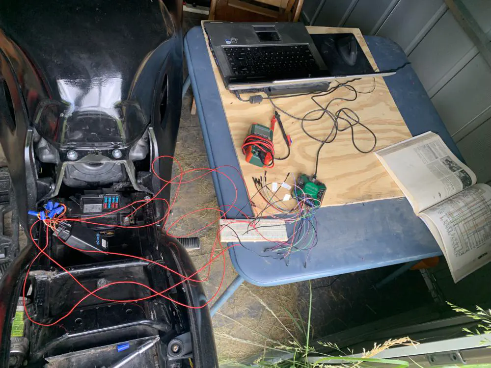
In a well-ventilated area, we’ll fire up the Katana and take a look at the oscilloscope:
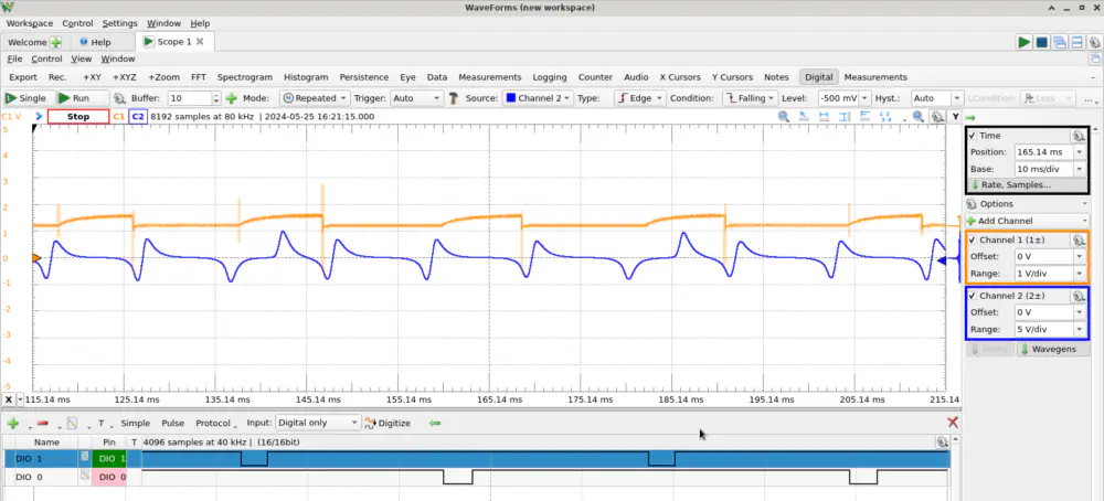
Nice! The yellow line shows the throttle body which was mostly held constant with a few jitters (potentially being moved slightly by air getting sucked around the throttle body). The blue line shows the output of the pulse generator. It seems to send four pulses each camshaft revolution. Three of them are uniform, but one has its timings altered a bit to help the ignition control system match which pulse is which angle.
Below the analog graph, we can see active-low pulses to the digital pins from the ignition control system as it triggers the two coils.
Building the Simulation Hardware
To power the ignition control system, I used a 12V power supply to emulate a battery. From here, I could start building up the input and output circuitry.
When looking at the pulse generator inputs on the ignition control system, I noticed that one of the wires was actually held to ground. This likely means there is a diode to only allow the positive pulses from the pickup coil since the negative voltages would be negative for the microcontroller as well (which would damage it). Furthermore, I assumed it was only looking at rising and falling edges so I could simply write digital pulses to the wire that wasn’t grounded and I would be good to go.
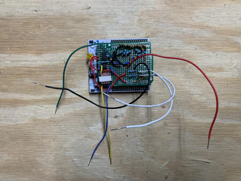
For whatever reason, I could not get this to work and had to resort to actually emulating those pickup pulses as well as I could. For this I first switched from an Arduino Uno to a NUCLEO-F070RB board. I needed something with a higher clockspeed to smoothly emulate the pickup coil pulses at higher RPMs. There are board configurations that let you write code for the STM32 microcontroller on the NUCLEO board using the Arduino IDE. The board also has headers that match up with Arduino Uno headers so I could use my shield protoboards on it.
The next problem is: how am I supposed to generate negative voltages? I wanted my circuit to have the same ground as the ignition control system because anything else would be a lot more messy and complicated. What I ended up doing was building a 6-bit digital-to-analog (DAC) converter using a resistor ladder. This let me take 6 pins from the NUCLEO board and convert it to an analog signal that could output 64 different voltage levels from 0-3.3V. I took that output and connected it to a voltage follower using an operational amplifier. I then used another resistor ladder to produce a constant 1.65V and used that as the input to another operational amplifier voltage follower.
I connected the outputs of the operational amplifiers to a small 1:1 audio transformer. By doing this, I was able to generate an AC voltage from -1.65V to +1.65V on the other side of the transformer and connect that up to the pulse generator wires on the ignition control system.
The throttle input was much simpler, here I built another 6-bit DAC, amplified it from 0-3.3V to 0-5V using another operational amplifier and put the output into the throttle body position sensor wire.
For outputs, I used the 12V output from the power supply across 1K ohm resistors to the two coil control wires. When the control wires were inactive, they would stay at 12V, but when they were active the wires would drop to nearly 0V. I used much higher ohm resistors to make a voltage divider so that when the wires were at 12V, a 3V signal was going into the NUCLEO’s analog 0 and analog 1 inputs. By detecting voltage drops on A0 and A1 of the NUCLEO board, I could now detect the ignition control system’s coil pulses.
Here is the NUCLEO board with my protoboard on top of it.
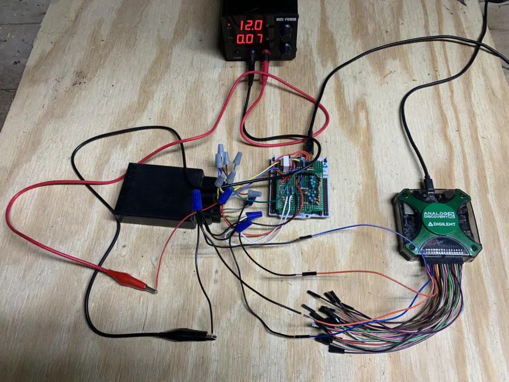
Here is the power supply (top), the ignition control system (right), the NUCLEO board/protoboard (middle), and the Analog 2 (right) to help troubleshoot.
Programming the Simulator
The main idea was to write code for the NUCLEO board that would read a timeseries of RPMs and throttles over serial from the computer. After the NUCLEO finished emulating the timeseries, it would send ignition timing information back to the computer over serial.
On the computer, I ran Python programs that sent different combinations of timeseries to the NUCLEO and output the results in CSV format.
Finally, I used a Jupyter notebook with Matplotlib to help me analyze the outputs. Here is a scatterplot where I iterated over a range of throttle values from 0 to 63 (remember, it’s a 6-bit DAC) and RPMs from 300 to 18,300 at 500 RPM increments. Then I calculated the average timing for each coil as a floating value between 0 (the beginning of the camshaft’s rotation) and 1 (the end of the camshaft’s rotation).
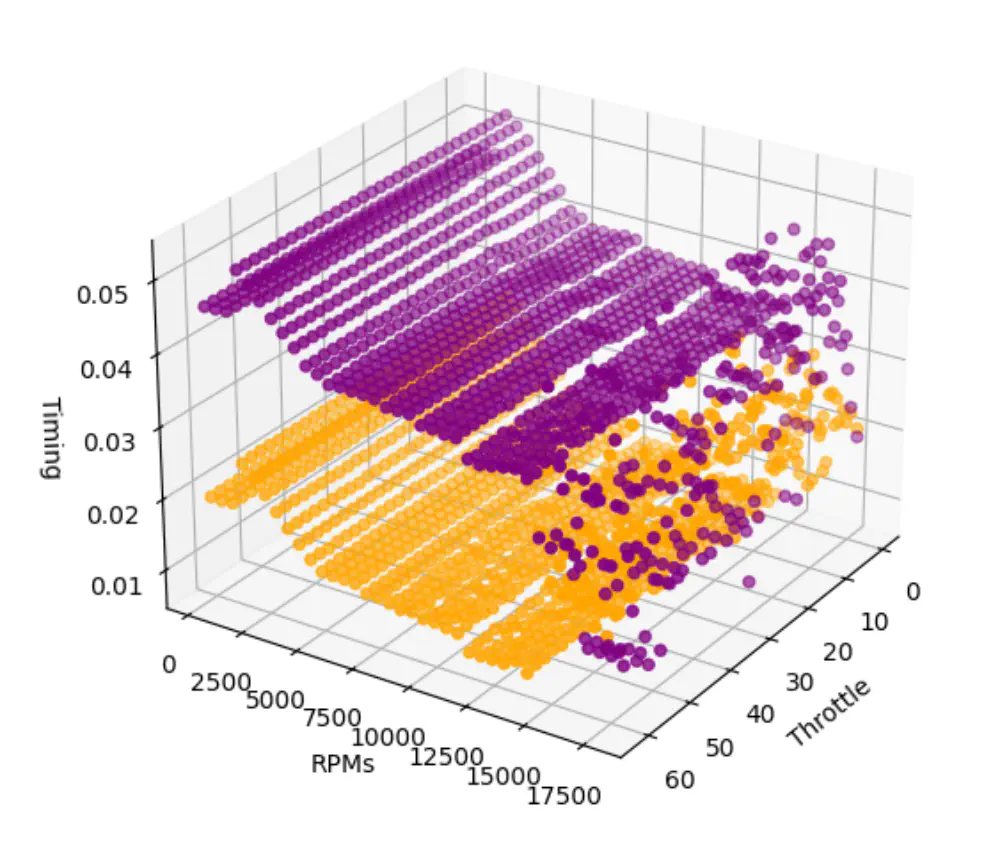
From the scatterplot, we can see that at lower RPMs the timing is fairly constant. Then at ~3000 RPMs it increases the timing, then gradually decreases as RPMs or throttle increases. However, once the throttle exceeds 15,000 RPM (the rev limit), the ignition control system starts skipping ignitions to try to slow the engine down. Because of how I am calculating/averaging ignitions the points become inconsistent and scattered along the Z (Timing) axis.
At this point we have reverse engineered the ignition control system well enough to start building something new. With the ignition timing information I can begin to write my own algorithms on a more modern microcontroller to match how the ignition control system behaves or tune it for more power or more efficiency.
Conclusion
My adventure started with hopes of finding a debugging interface on an ignition control system and ended with building an entire hardware simulator. There were a lot of setbacks along the way like not being able to reprogram the microcontroller or even read its firmware directly. But in the end, I was able to get the precious timing information I wanted and in the middle I learned about:
- The Background Debug Mode (BDM) protocol.
- Probing circuit boards and identifying components.
- Identifying an unknown microcontroller.
- Blackbox testing at a hardware level.